Intel CEO Pat Gelsinger today launched Intel Foundry as a sustainable systems foundry business designed for the AI era.
The word “foundry” means that Intel will make chips designed by other companies, and it is spending billions of dollars upgrading its manufacturing capacity and designing its manufacturing nodes to keep up with the needs of external chip designers. Gelsinger believes that this huge investment is necessary to take the AI boom to its next level.
Years ago, Intel was the world’s biggest chip maker and it did a fine job keeping its factories humming with chips designed by Intel engineers. But times are different now, with rivals such as Nvidia and Advanced Micro Devices making gains on chip design while TSMC and Samsung are commanding big chunks of the chip manufacturing market.
Gelsinger wants to beat those companies with IDM 2.0, a strategy that refers to “integrated device manufacturer” where Intel both designs chips and makes them too. Most other chip makers can’t afford factories and have chose to farm out the manufacturing to the likes of TSMC and Samsung. This strategy represents a doubling down on what Intel used to do so well — before Intel’s prior CEO lost focus and the board had to bring Gelsinger back to his former company, this time as CEO, in 2021.
GB Event
GamesBeat Summit Call for Speakers
We’re thrilled to open our call for speakers to our flagship event, GamesBeat Summit 2024 hosted in Los Angeles, where we will explore the theme of “Resilience and Adaption”.
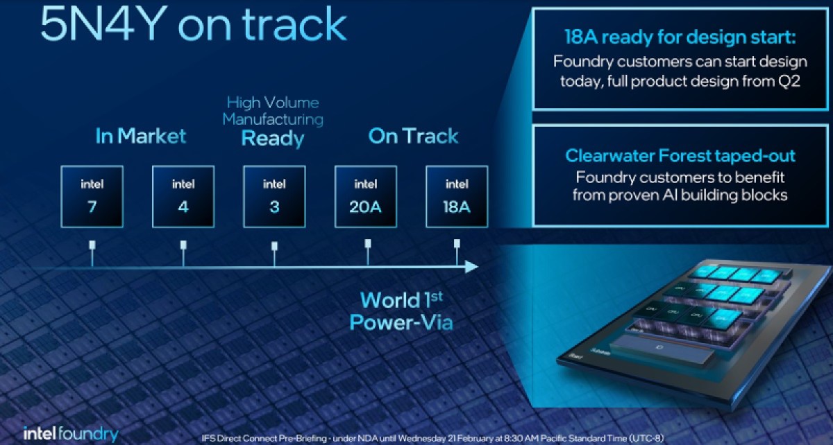
Today, Intel is talking about what comes next after its monumental feat of creating the 18A manufacturing process and developing five manufacturing nodes in four years in a bid to say that “Moore’s Law” isn’t dead. With AI driving demand for high-end chips and the U.S. government funding chip manufacturing through the CHIPS Act, Gelsinger’s bet has a very good chance of paying off.
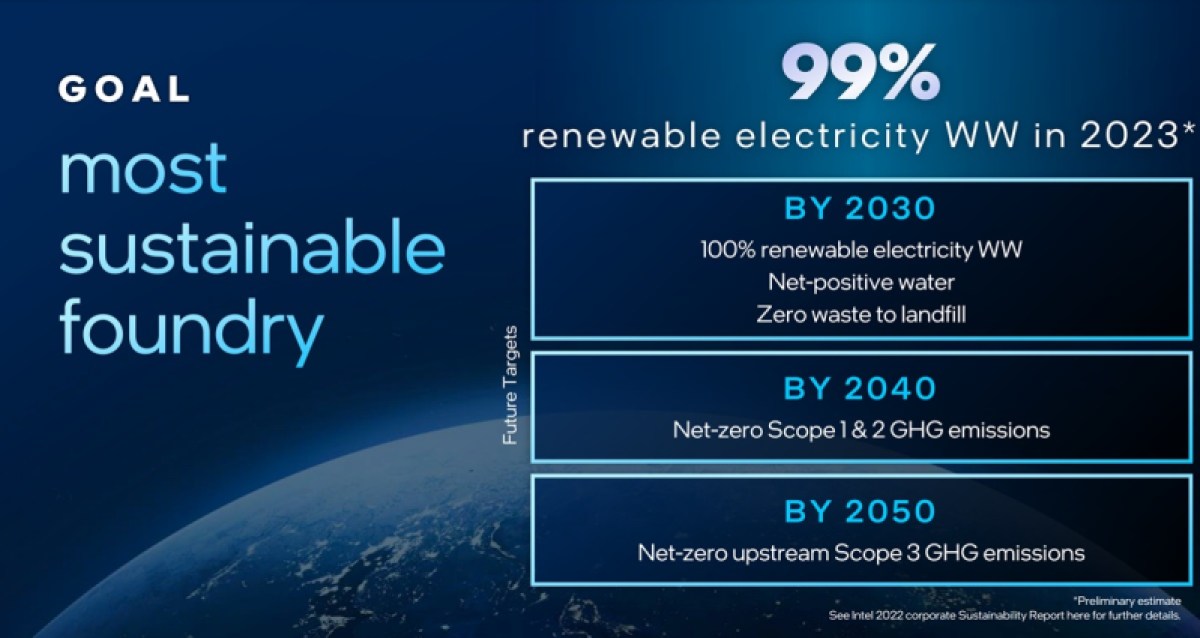
Gelsinger said Intel is on track to do five nodes in four years and it is adding a new node, Intel 14A, and other evolutions of nodes for the future. It also plans to set the standard for foundry sustainability with renewable electricity usage.
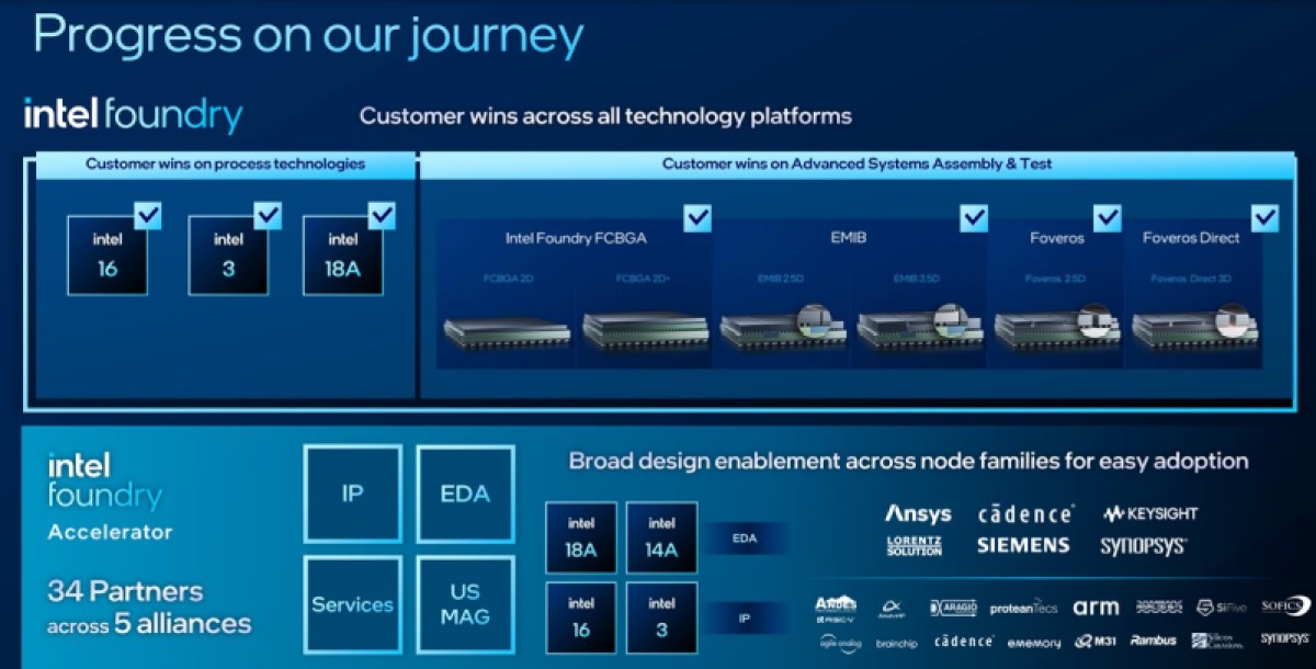
Intel announced new customers for the foundry business and an expanded process roadmap that aims to establish itself as the process technology leader in the latter half of this decade. It announced partnerships with Arm, Synopsys, Cadence, Siemens and Ansys — as it prepares tools, design flows, and IP portfolios validated and ready to enable customer designs.
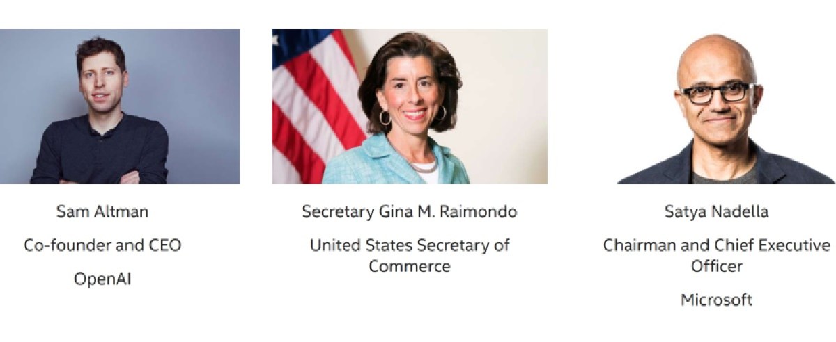
Intel announced its news at its first foundry event, Intel Foundry Direct Connect, where it gathered customers, ecosystem companies and leaders from across the industry. Among the participants and speakers were U.S. Secretary of Commerce Gina Raimondo, Arm CEO Rene Haas, Microsoft CEO Satya Nadella, OpenAI CEO Sam Altman and others.
Here’s an edited transcript of our interview.
VentureBeat: Tell us about your big event.
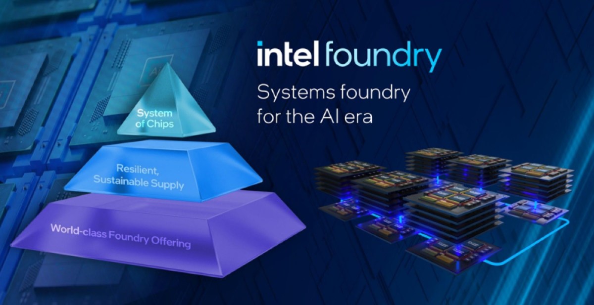
Patrick Gelsinger: This is a key moment in the progression at the Intel foundry. We view the opportunity to position what we call the Intel Systems Foundry. A systems foundry, we believe, is a significant move from just being a wafer provider, to delivering a whole range of technologies – wafers, packaging, systems and software capability. With the surge of AI we see that the capabilities that Intel brings to the table are significantly greater than just the wafer foundry as that category has been defined today.
Also, the process technology is making major steps forward, delivering on our five nodes in four years road map. But also, for the first time, we’ll be laying out what’s next, laying out the broadening of the portfolio of capabilities. With that will be what’s beyond 18A. We’ll be describing the next nodes after that. 14A continuing to be a cadence beyond that, but also broadening the portfolio, adding variants to the Intel 3, extending the life of that. We’re also going to describe that Intel 3 is becoming a great base die. Wafer to wafer assembly, chiplets on top of a base die. This will be a key technology, and so we’ll announce Intel 3T, and other enhancements to 18A for a broadening of that node.
We’ll also be describing the Intel Foundry. We’ll give a name to TD manufacturing and IFS, naming that as a new group for Intel, and Intel Foundry as a collection of those capabilities coming together. We’ll also be describing an expansion of the ecosystem. The broadening of the availability of the EDA tools, as well as IP providers that will be part of our activity. We have strong messages from both the EDA providers and IP providers like ARM as part of it. They’ll be giving updates on how they’re taking advantage of Intel technologies and bringing those forward more broadly.
Collectively, the set of announcements is really a coming-out party for the industry. The world is looking forward not to just a more sustainable, resilient supply chain, but also delivering on this message of the systems foundry for the AI era.
VentureBeat: How did you come to the conclusion about what Intel needs to own? We have TSMC on the one hand and Nvidia doing a different strategy. Why decide to own the manufacturing and try to differentiate on that front?
Gelsinger: To a great degree, Intel has been a manufacturer forever. I talked about IDM 1.0. As we announced our IDM 2.0 strategy a little over two years ago, it was really becoming a world-class fabless company and a world-class foundry. The unique ability we had to create more scale and efficiency by being a foundry for the industry. Obviously the AI surge created this moment in time where–what I call our advanced packaging is a capability that Intel has been a leader in forever. With that now, these advanced AI components need advanced packaging. It’s been a tail wind for our move into foundry.
We’ve been good in this area. Now, with the surge in AI, we’ve gotten a bit lucky as well. We’re seeing a lot of momentum there to accelerate the overall foundry customer engagement. Clearly, as we execute on our strategy, as we’re getting 18A done and laying out that road map, we’re getting more and more interest from major customers taking advantage of western foundry.
VentureBeat: If I look at OpenAI, they want to raise these trillions of dollars. You definitely want some of that to go to Intel.
Gelsinger: We’re building major factories for everyone in the world.
VentureBeat: There are companies that are interesting in the customer space now, too. The Ciscos, Amazons, Googles, Metas. They don’t necessarily want a middleman to design for them. They do design themselves. But they need someone to make it for them. This is an opportunity there.
Gelsinger: Unquestionably. We’ve already been working with Amazon, for instance, as a packaging supplier. That’s an area where they want to work with us. Many companies doing their own chip designs want a broadening set of technologies. The ability for Intel to step in to be a broader supplier–clearly, we have Gina Raimondo participating in the event, reinforcing the criticality of the support from the U.S. government to build the western foundry and more manufacturing capacity on American soil.
The world needs a balanced and resilient supply chain. Everything relies on semiconductors. In that context, there’s only essentially two or three sources in the world for leading-edge logic technology. The fact that we have logic technology, we have systems capability, we have advanced packaging–it really does give us this AI-era systems foundry capability in a very unique way.
VentureBeat: It seems like you’re taking different kinds of stands here. Where you build it matters. What you own matters. Where the line is between something more open and something more closed–the point at which you decide to draw that is an important decision.
Gelsinger: Intel has had many of these technologies for many years. Many of our packaging technologies–we’re now opening the doors wide. We’re taking the best of Intel’s capabilities, and in many cases–next week we’ll describe our next-generation Clearwater Forest, the first 18A server chip. We’ll describe in detail its construction, and present all of those technologies to foundry customers. We’re customer zero. We’re driving the innovation of many of these technologies. But this idea of chip-on-chip, packaging, the capabilities that we’re using to construct what we believe is the unquestioned best server chip in the world, we’ll bring that to the fore. We’re also saying that every one of those component technologies is available for third parties working with the Intel foundry.
This, I think, is the unique capability that Intel is presenting, the best of both worlds. Here’s how we’re de-risking that, innovating with our product offerings and making them available to every foundry customer in the world. Something we’ve never done before. This is what it means to be IBM 2.0.
VentureBeat: Another CEO has been talking about sovereign AI. Where your data is matters. You’re also saying that there’s sovereign chip manufacturing. Where those chip factories are matters.
Gelsinger: Yeah, unquestionably. With that, why is Gina Raimondo participating? Because she believes that through the CHIPS Act, Commerce wants to see more of this built in the U.S. They’re strongly supporting the buildout of the resilient supply chains for the world. As I say, there should not be one source of leading technology. Given that many of these chips are designed in the U.S., and much of the AI innovation is occurring in the U.S., we believe that the supply chains for that should be in the U.S., and in Europe as well. It’s the right thing for an increasingly digital world, to have resilience and geographically balance the supply chains.
VentureBeat: Different people have pointed out that Intel has gone this route before. Why is it different now?
Gelsinger: A couple of things. One is that those earlier efforts–Intel was, I’ll say, pretty proprietary at the time. It was a big hurdle for people to use the Intel technology. We’ve now embraced the ecosystem very aggressively. That’s having Cadence, Synopsis, Siemens there, plus many of the IP providers like ARM. They’ve seen Intel become industry standard. The industry is able to join – and we’re able to join the industry – in an open and standard way, something we didn’t do before.
Second is, I’ve committed the Intel strategy to this. Before, as I call it, it was a sort of hobby on the side. Now I’ve centered the Intel strategy. I’m restructuring the company with this in mind. We are rebuilding and we’ll be presenting, in the next quarterly earnings call, the first ever unique financials. We’re running technology, manufacturing, and foundry as a P&L. I’ve fundamentally changed the operations of the company to make this not a hobby, but the center of how we run our operations. I’ve centered our strategy on it. I’m rebuilding the company to do this.
We’re already way beyond in terms of the revenues that we’re seeing, the bookings that we’re already committed to. We’re already far more progressed than we ever were before. Early on I think people might have had that skepticism. Now look at what we’re doing, the revenues we’re committing to. We’ve talked about lifetime deal value. We’ve already gone way past some of those early projects in the developer of the strategy and the execution.
VentureBeat: What’s your feeling about Moore’s Law and where we are on that? Does this help or otherwise complicate that?
Gelsinger: I’ve said that Moore’s Law isn’t over until we’ve exhausted the periodic table. But we deeply believe that innovation in Moore’s Law is still alive and well. We present power, performance, area increments that we’re able to achieve. We feel confident that we can continue progressing on Moore’s Law.
There are four reasons we believe that’s feasible for at least the next decade, if not beyond. Number one, the advancements in lithography. EUV, the next generation, high NA. We can make transistors smaller and smaller. Second is backside power. We’re able to continue to drive area improvements. Third, gate-all-around. A major new transistor structure. Fourth, this idea of going to 3D silicon with advanced packaging. We’re no longer just innovating along X and Y. We’re innovating along X, Y, and Z. The combination of which–we think we hit a trillion transistors by the end of the decade, which is nominally going from 100 billion in an advanced package product up to a trillion at the end. That’s essentially right on the money for Moore’s Law this decade. We believe we’re on track to deliver it because we’re advancing on all four of those dimensions.

VentureBeat: You’re not exactly talking about customers yet, but maybe dropping some clues?
Gelsinger: We’ll be updating on the customer front. As we said on the last earnings call, customers are reluctant. They have a major supplier. It’s also not customary in the foundry industry to describe your foundry suppliers that you have. We’ll be updating as more customers give us authority to use their names. But we’ve also said that we’ll update on measurements like lifetime deal value as a way that the market can measure our progress in this respect.
We’ll give as much information as we can. Given the reluctance of customers and the concentration of the industry and its practices, we may or may not be able to give names as much as some might like. But we’ll give as much information as we can about the progress we’re making.
VentureBeat: I feel like this answer has been given across many categories of technology now, but there’s that question of, how is AI going to improve all of this and make it easier for you to stay on Moore’s Law? Also, how is AI going to change the structure of how things are done and what chip companies are going to look like?
Gelsinger: We’ll touch on one of these next week at the event. I see there are at least two different dimensions to this. AI is going to allow us to design more effectively. We’re putting AI into the chip design process. We’re not discussing in detail, but you can certainly hear from the EDA vendors, how they’re using AI techniques in their design tools. We’re using it in areas like, how do we drive signal integrity? How do we accelerate RTL development and those types of things using AI? There’s a lot of that going on, but we’re not particularly digging into that next week.
The thing that we will lay out is how we’re bringing AI techniques into the manufacturing itself. With that there will be things like–every image is now being analyzed because AI enables us to do that. This accelerates things like defect detection, yield enhancement, equipment maintenance management. We’re also introducing essentially “cobots.” Much more robotic automation in the manufacturing process as well, allowing us to increase the productivity and efficiency of the manufacturing itself. How do we deliver the most automated factories that have ever been created in the area of semiconductors? We’ll be describing some of the vision for that next week. Some of those techniques are already producing quite substantial enhancements that we’re seeing, where we’re able to predict yield variations more effectively, improve fin splits in products more effectively, and be able to drive the maintenance cycles of equipment more efficiently.
VentureBeat: Would you say that AI helps you get the benefits of a node change without the node change?
Gelsinger: You’ll hear from one of the EDA vendors next week, and you’ll hear them describe exactly that.
VentureBeat: Is that in some way how you get to five nodes in four years, or is it building on top of those node gains?
Gelsinger: I would say it accelerates–not so much how we get to five nodes in four years. That’s much more chemistry and physics and so on. Some of that is being enhanced by AI techniques, but a lot of that is hardcore innovation, catching up, capital investments, and so on. However, getting more designs migrated to 18A, that’s very much taking advantage of these AI techniques. We’re able to take designs that were done on other foundries and accelerate their movement onto Intel’s foundry as a result.
VentureBeat: It sounds like Intel is speaking the language of broader ecosystems, more partners, and more openness. Does that go hand in hand with these different eras we have, the AI era and this new focus on the foundry era?
Gelsinger: Simple answer, yes. Some of these, I’d say, are traditional things we’ve done. Intel drove PCI-e, an inter-component standard. Now we’re driving UCI-e, a chiplet interface standard. Every analogy you might have in mind was exactly what we would intend. When you look at an advanced packaging part, what’s the interface between these pieces of silicon? We’re standardizing on UCI-e so we can intermix different chiplets together.
Some of this, as you said, is going to industry standard tools and techniques, like standard PDKs that the industry is familiar with from the foundry world. This is something we’ve never done before. Now we’re delivering industry standard collaterals for people to design with and EDA vendors to take advantage of. All that, I’d say, means yes, we’re becoming much more industry standard, as well as through the foundry strategy, making those available at the individual technology level. Our packaging technologies, the chiplet technologies, the system components, we really are coming with an open hand to the industry and saying, “Take advantage of the best that Intel offers.”
VentureBeat: There’s a piece here where you compete like hell to have the most unique thing that people need from you, even though there’s also that openness and shared ecosystem.
Gelsinger: Absolutely. On the product side, their job is to build the best products, period. Fight for market share every day of the week. But on the foundry side, build the best process technologies, the best packaging technologies, and fight like crazy to win every wafer, every packaging, every socket you can. It’s those two pieces of the business that are the basis of IBM 2.0. Restructuring the company to present being a world-class foundry and a world-class product provider.
If we come back to the starting theme of the discussion, I would say I’m the only company that has 100% of the AI TAM available. If you’re building your own chip, I want to be your foundry. I want to sell you my chip. Either way I want to participate in the AI market. I want to be the foundry for Nvidia and Broadcom and everyone else. And I want you to use Xeons and Gaudis and Core Ultras, our products. I want to participate in 100% of the TAM.
VentureBeat’s mission is to be a digital town square for technical decision-makers to gain knowledge about transformative enterprise technology and transact. Discover our Briefings.