Shortwave infrared light (SWIR) sensors are desirable in a broad range of applications, particularly in the service robotics, automotive, and consumer electronics sectors. Colloidal quantum dots tuned to SWIR show promise for such sensors since they can be easily integrated into CMOS, but their mass market use has been hampered by the fact that most contain toxic heavy metals like lead or mercury. Now a team of scientists has manufactured quantum dots out of non-toxic materials and tested them in a fabricated lab-scale photodetector, according to a recent paper published in the journal Nature Photonics.
“SWIR light for sensing and imaging is of paramount importance owing to its unique characteristics,” the authors wrote. “It is eye safe; it can penetrate through fog, haze, and other atmospheric conditions, enabling imaging under adverse weather for automotive applications, environmental, and remote sensing; the presence of night glow under night in the SWIR range enables passive night vision; and visual imaging combined with infrared spectroscopy enables machine vision, bio imaging, and food and process quality inspection,” among other applications.
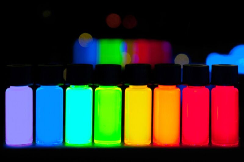
As previously reported, a quantum dot is a small semiconducting bead a few tens of atoms in diameter. Billions could fit on the head of a pin, and the smaller you can make them, the better. At those small scales, quantum effects kick in and give the dots superior electrical and optical properties. They glow brightly when zapped with light, and the color of that light is determined by the size of the quantum dots. Bigger dots emit redder light; smaller dots emit bluer light. So you can tailor quantum dots to specific frequencies of light just by changing their size.
Once thought impossible to make, quantum dots have become a common component in computer monitors, TV screens, and LED lamps, among other uses. For instance, quantum dots allow TV manufacturers to precisely tune the emitted colors, producing more accurate hues over a wider range, all while using less electricity. They’re useful as an alternative to the organic dyes used to tag reactive agents in fluorescence-based biosensors and have been incorporated into glass windows to essentially turn those windows into photovoltaics, potentially harvesting small amounts of solar energy to offset home energy costs.
In 2013, German physicists built the experimental equivalent of Maxwell’s demon with a pair of interacting quantum dots. In 2015, scientists made quantum “pee-dots” out of recycled urine and used them to bio-image mouse cells. Future applications might include incorporating quantum dots into flexible electronics, tiny sensors, and solar cells or using them in encrypted quantum communication systems.

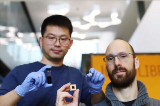
The authors of this latest paper hail from the Barcelona Institute of Science and Technology (BIST) and Qurv Technologies in Spain. The BIST team was looking into ways to synthesize silver bismuth telluride nanocrystals for photovoltaic devices and noticed that silver telluride was one of the byproducts. The silver telluride had properties ideal for colloidal quantum dots, most notably tunability. So the team switched course and developed a process for making silver-telluride quantum dots.
The resulting quantum dots had a good size distribution and were tunable over a broad spectral range, including SWIR. The next step was to incorporate those quantum dots into a lab-scale photodetector. It was a challenge to revert the usual device setup since one shines light from the bottom of most lab-scale devices, while CMOS-integrated CQD stacks involve shining light from the top, with the CMOS electronics on the bottom. The first attempt was only moderately successful because the resulting photodiode didn’t perform as well as expected in the SWIR range.
The BIST researchers redesigned the sensor with an additional buffer layer to fix the issue, resulting in a much more effective SWIR sensor. They then collaborated with Qurv scientists to construct a proof-of-concept SWIR image sensor made of non-toxic quantum dots operable at room temperature. They were able to capture images of the silicon wafer transmission under SWIR light and peer inside plastic bottles that are opaque under visible light. The next step is to re-engineer the stack of layers to further improve photodiode performance, as well as exploring other surface chemistries.
Nature Photonics, 2024. DOI: 10.1038/s41566-023-01345-3 (About DOIs).
Non-toxic quantum dots for CMOS shortwave infrared image sensors for consumer electronics.

