In 2019, AMD introduced a new GPU architecture, marking its first major graphics chip design in seven years. Since its debut, this architecture has seen two revisions, emphasizing the significance of chiplets and cache in the rendering arena. Given these developments, it’s pertinent to assess what AMD has accomplished with its engineering prowess and to consider the impact of each update.
We will explore the technology that was unveiled, assess its performance in games, and examine its financial implications for AMD.
Has RDNA become as monumental a success as Zen? Or have the various modifications led to another “Bulldozer” moment for AMD? Let’s find out.
Why GCN needed to change
Current AMD GPUs fall into one of two distinctly separate product sectors – those that are targeted at gaming and those that end up in supercomputers, big data analyzers, and machine learning systems.
They all, however, share the same heritage – an architecture known as Graphics Core Next (GCN). This first appeared in 2012 and remained in use for nearly 10 years, albeit with some heavy revisions along the way. GCN was a thorough overhaul of its predecessor, TeraScale, and from the ground up, it was designed to be highly scalable and equally at home in graphics and general-purpose compute (GPGPU) applications.
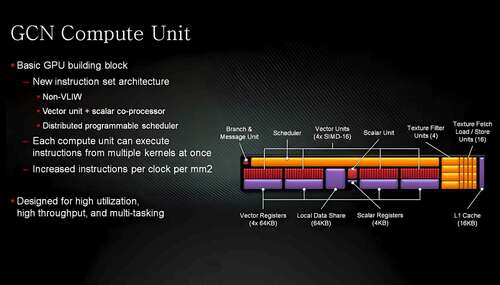
The scaling side of things came from the way that the processing units were grouped together. From the very first version of GCN to its final revision, the foundations of the GPU comprised a block of 4 Compute Units (CUs).
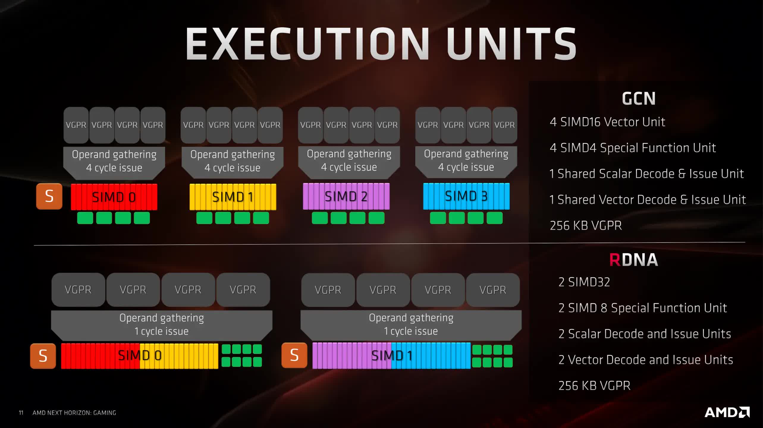
Each of these housed 4 SIMD (single instruction, multiple data) vector units that carried out math operations on 16 data points, 32-bits in size, and a single Scalar unit which was used for integer-based logic operations.
Each vector SIMD had a 64 kB register file and all four units shared a 64 kB block of scratchpad memory (called the Local Data Share, LDS) and all of the processing units shared a 16 kB L1 data cache. The quad group of CUs shared a 16 kB scalar cache and a 32 kB instruction cache, with all of these caches being linked to a GPU-wide L2 cache.
By the time GCN 5.1 came around in 2018, none of this had changed much, though there were multiple improvements to how the cache hierarchy operated. For the world of gaming, though, GCN had some notable shortcomings, but they can be summarized in that it was a challenge for developers to get the best performance from the chips, in terms of processing throughput and bandwidth utilization.
For example, threads were dispatched by the GPU in groups of 64 (each called a wave or wavefront) and every SIMD unit could be issued with a different wave, queued up to 10 deep. However, the issue rate of instructions was 1 every 4 cycles so to ensure the units were kept busy, lots of threads would need to be dispatched – more than achievable in the world of compute, far less so in gaming.
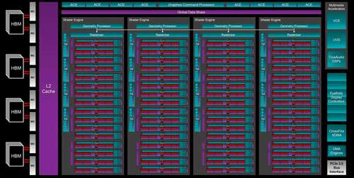
The first version of GCN boasted hardware structures called Asynchronous Compute Engines (ACE). When it comes to rendering a frame in a 3D game, the GPU is given commands by the system that are set out in a long queue. However, they don’t all need to be done in a strictly linear sequence and this is where the ACEs came into play.
GCN-powered GPUs could essentially split the queue into three different types (one each for graphics commands, compute work, and data transactions), and then schedule them accordingly. At the time, though, the Direct3D API didn’t have much support for this system, though once Direct3D 12 was released in 2015, asynchronous shading became all the rage. AMD capitalized on this by making GCN even more focused on compute.
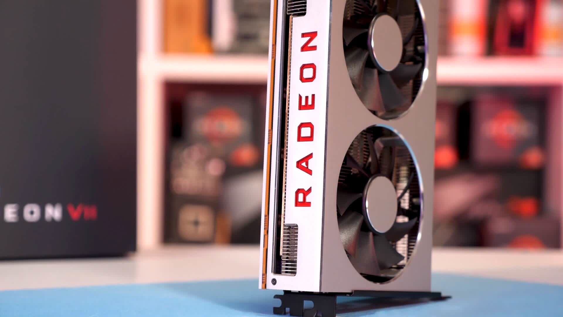
This was blatantly clear with AMD’s last hurrah for GCN in the high-end gaming graphics card market, the $700 Radeon VII (below). Sporting 60 CUs (the full chip had 64 of them) and 16 GB of HBM2 memory on a 4096-bit wide bus, it was an absolute monster of a GPU.
Against the GeForce RTX 2080, which also launched at $700, it could be faster in some games, but the majority of benchmark results showed that the architecture just wasn’t ideally suited for the modern world of 3D gaming.
GCN 5.1 was primarily used in professional workstation cards and the Radeon VII was essentially nothing more than a stop-gap product, created to have something on shelves for gaming enthusiasts, while the next generation of GPUs was getting ready to make an appearance.
Just four months later, AMD released its successor to the long-running GPU architecture – RDNA. With this new design, AMD managed to address the majority of GCN failings, and the first graphics card to sport this architecture, the Radeon RX 5700 XT, clearly highlighted how much more it was tuned towards gaming than GCN was.
One small step for GPU-kind
When the Ryzen series of CPUs in 2017, with the new Zen design, buyers were treated to a completely new architecture, built afresh from the ground up. This wasn’t the case with RDNA, as the fundamental concepts were still GCN-like in nature. However, pretty much everything inside was tweaked to make it easier for game developers to achieve the maximum possible performance from the GPU.
The SIMD count per CU was switched from 4 to 2, with each now working on 32 data points, rather than 16. The dispatch unit could now handle threads in batches of 32 or 64, and in the case of the former, the SIMD units could now be issued and process an instruction once per cycle.
These two changes alone made it significantly easier for developers to keep the GPU busy, although it did mean the compiler had more work to do in selecting the right wave size for processing. AMD selected 32 for compute and geometry shaders, and 64 for pixel shaders, though this wasn’t something that would be set in stone.
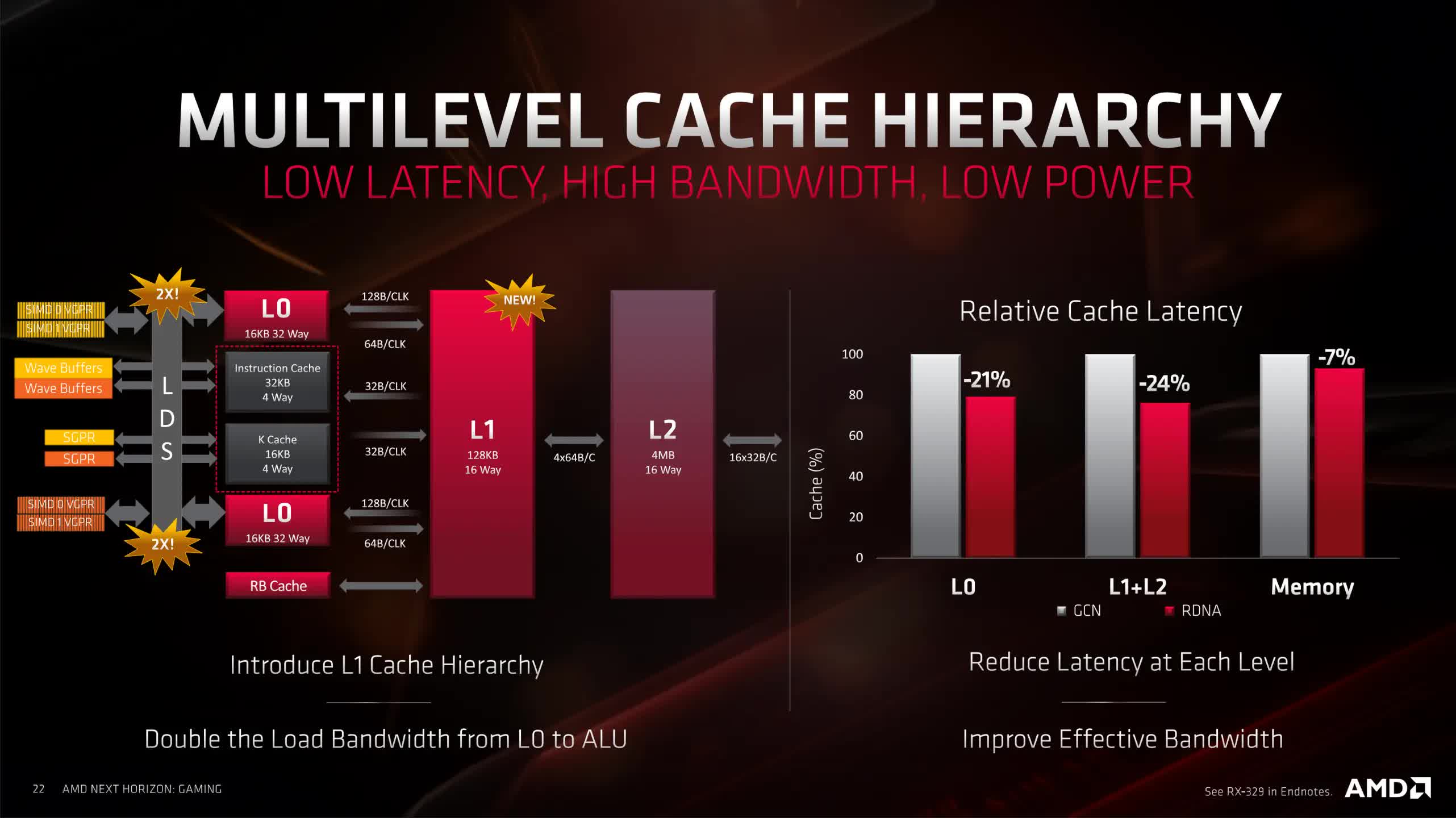
CUs were now grouped in pairs (called a WorkGroup Processor, WGP), rather than quartets, and while the instruction and scalar caches were still shared, they now only had to serve two CUs. The original 16 kB L1 cache was tweaked and relabeled as L0, and a new 128 kB L1 now served a bank of four WGPs – both sporting cache lines 128 bytes in size (helping to improve internal bandwidth utilization).
Lossless data compression was now used in every section of the GPU, latencies across the board were reduced, and even the texture addressing units were updated. All of these changes helped reduced the amount of time wasted by moving data about, flushing caches, and so on.
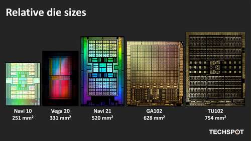
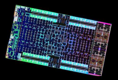
But perhaps the most surprising aspect of the first version of RDNA wasn’t the architectural changes but the fact that the first iteration of it was in a mid-range, mid-priced graphics card. The Navi 10 chip in the Radeon RX 5700 XT wasn’t a hulking slab of silicon, packed with Compute Units, but a mere 251 mm2 in size and 40 CUs inside. Made on the same TSMC N7 process node as the Vega 20 GPU in the Radeon VII, it was 24% smaller, which was great for wafer yields.
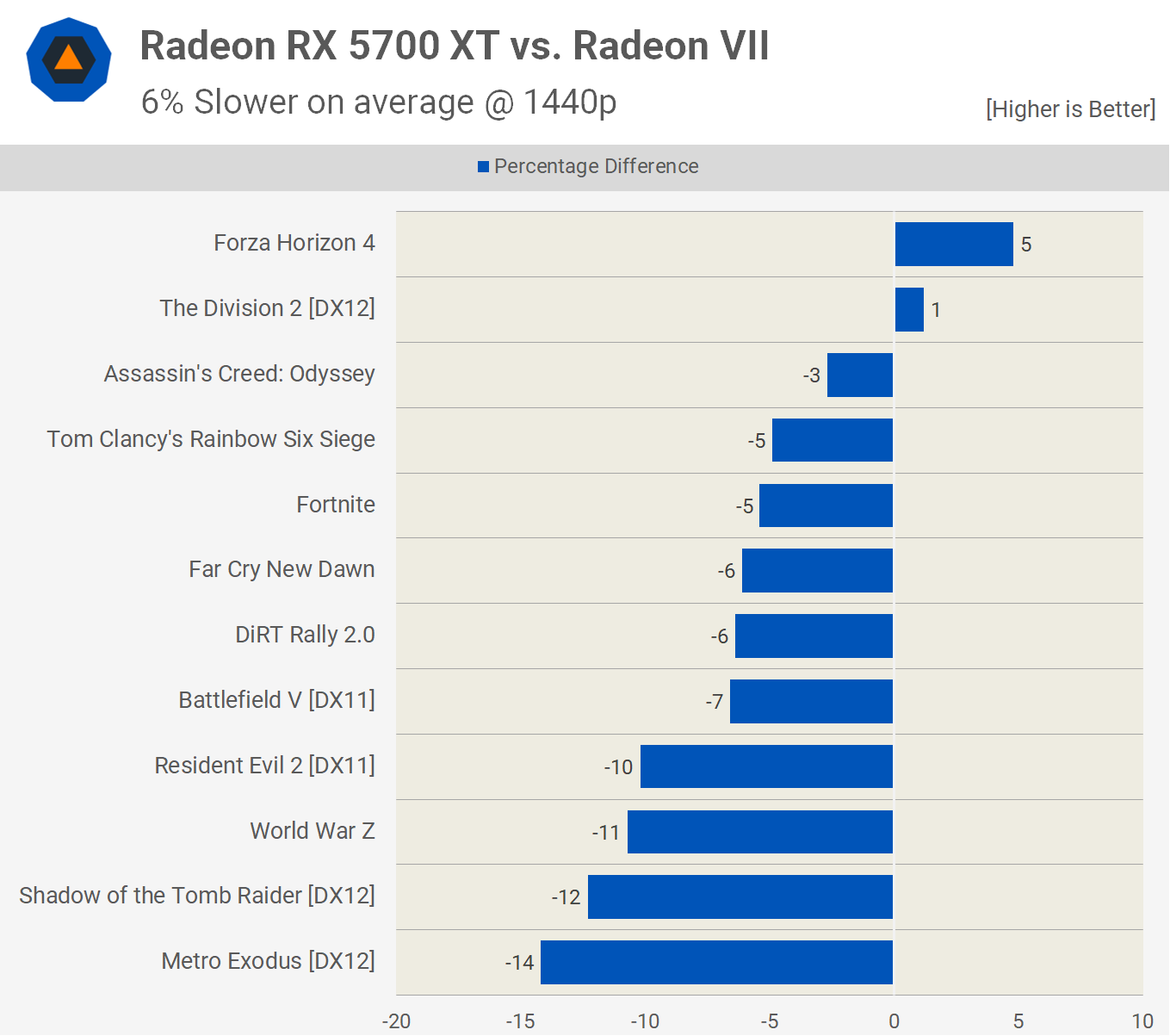
However, it also had 38% fewer CUs, though one couldn’t have expected all of the extra updates and cache to be free, in terms of transistor count. But when tested in games, it was only 9% slower on average than the Radeon VII and to top it all off, it was $300 cheaper.
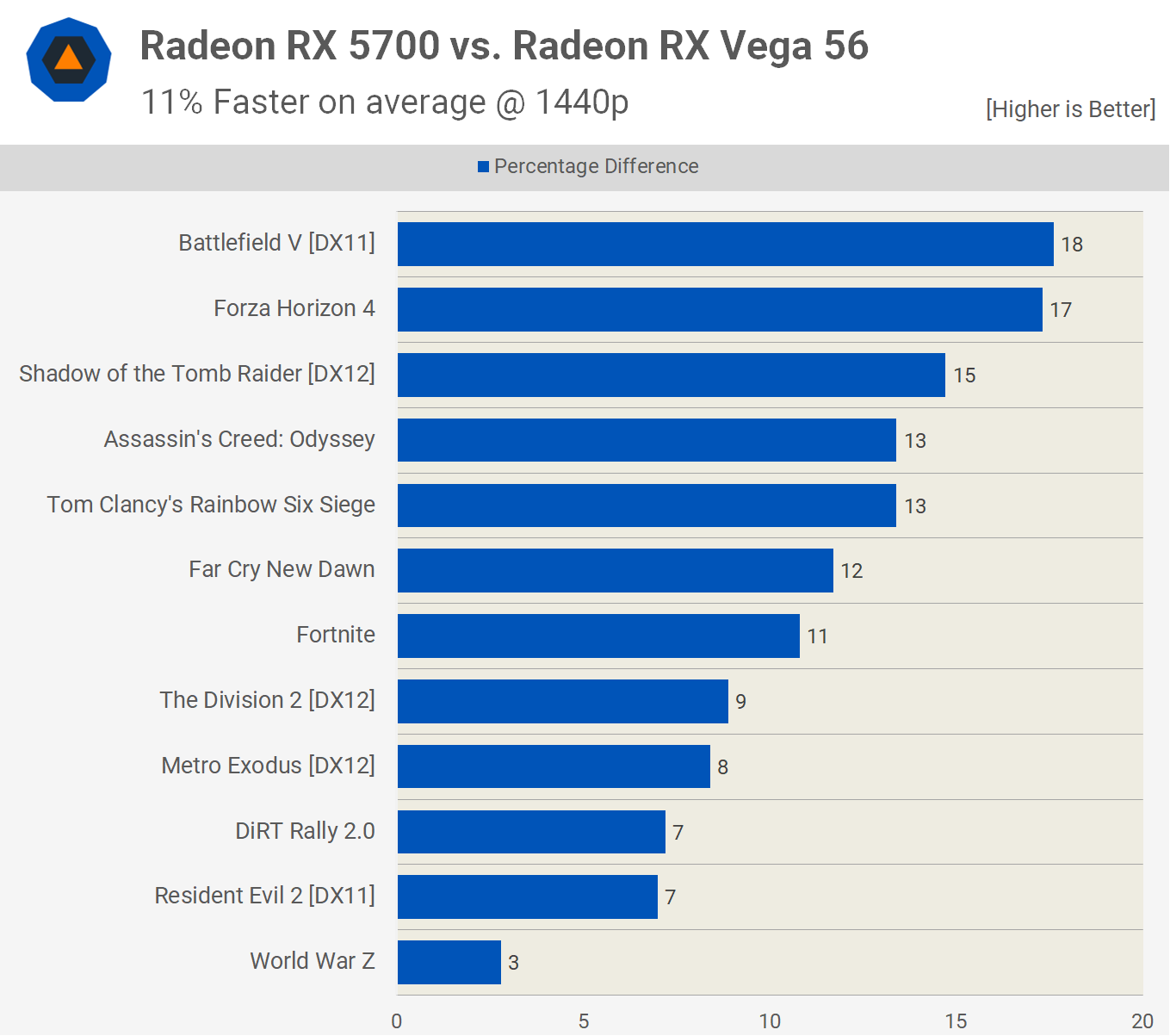
Overall it was a promising entry for the new architecture, as RDNA was a step in the right direction, albeit somewhat of a small one. With its performance being somewhere between the Radeon RX Vega 56 and the Radeon VII, it was a good balance of outright speed, power consumption, and retail price.
The launch of the new GPU wasn’t without issues, though, and while RDNA found a home in nearly 30 different products (through three variants of the chip design), some people were disappointed that AMD didn’t have something more potent for sale.
Fortunately, they didn’t have to wait long for that point to be addressed.
Round 2 for RDNA
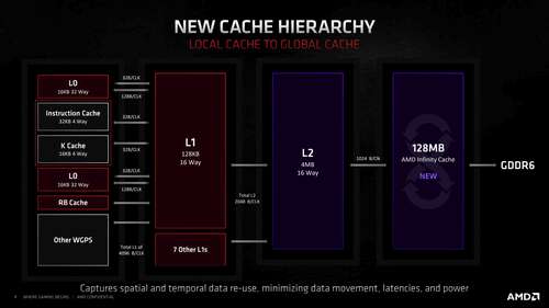
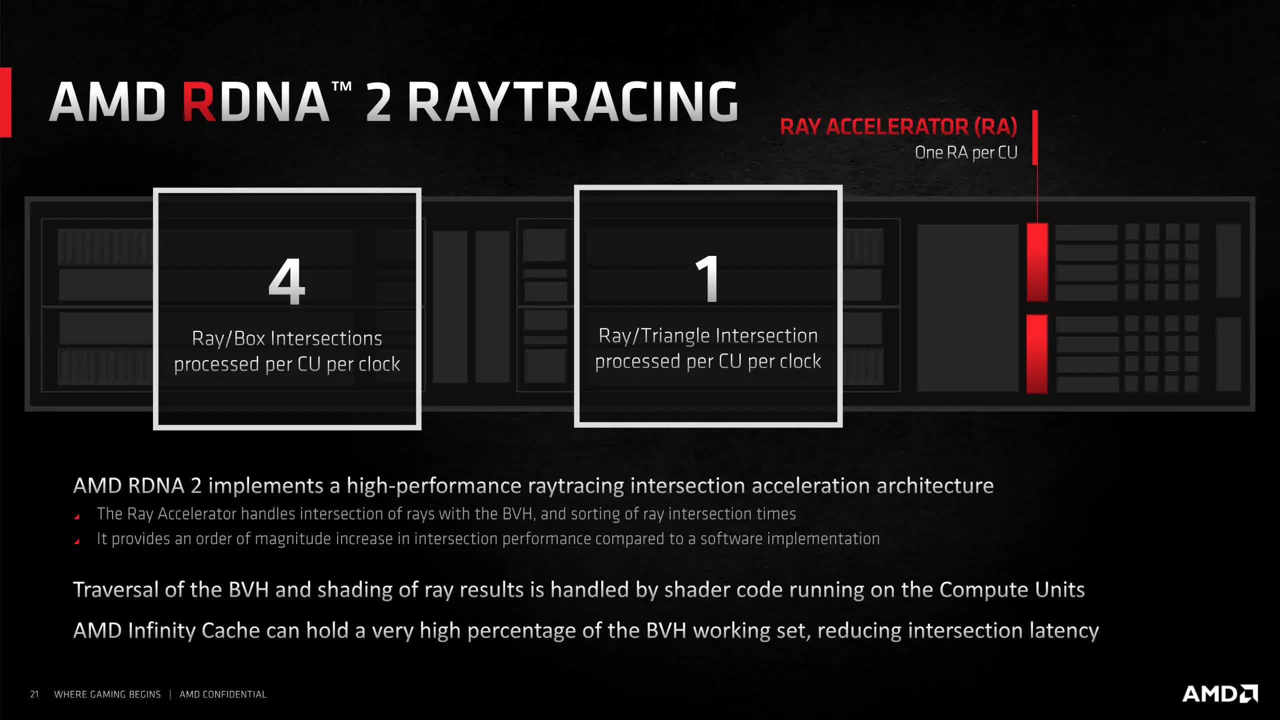
A little over a year after the Radeon RX 5700 XT launched, while the world was battling with a global pandemic, AMD released RDNA 2. On face value, almost nothing had changed apart from two new things – the texture units were upgraded so that they could perform ray-triangle intersection tests and an extra last level of cache (LLC) was added.
The former was a cost-effective addition to give the GPUs the ability to handle ray tracing, for the minimum amount of additional transistors, but the latter was no piecemeal offering, as it was far more than just a few MB. Up to that point in GPU history, 6 MB of LLC was considered ‘large’ so when AMD shoehorned 128 MB of it in the first RDNA 2 chip, the Navi 21, it not only stunned the GPU aficionados but it changed the course of graphics processors for good.
While processors had become ever faster and more capable, thanks to improvements in chip fabrication methods, DRAM was struggling to keep up. It’s much harder to shrink billions of tiny capacitors and not run into issues. Unfortunately, the more powerful a GPU is, the more memory bandwidth it requires to keep it fed with data.
Nvidia chose to go with Micron’s GDDR6X technology and festoon its GPU with lots of memory interfaces to get around this problem. However, this RAM was more expensive than standard GDDR6 and the extra interfaces just made the chips larger in size. AMD’s approach was to leverage its cache know-how from the CPU division and shove a mass of LLC into its RDNA 2 chips.
By doing this, the need for wide memory buses housing fast RAM was significantly reduced, all helping to keep GPU die sizes and graphics card prices under control. And die size was important here, as the Navi 21 was essentially two Navi 10s (so 80 CUs in total), all surrounded by a wall of cache.
The latter was built out of 10.3 billion transistors, whereas the new chip housed more than double this figure – 26.8 billion. The extra 6.2 billion was primarily being used for the so-called Infinity Cache, though there were other changes under the hood. AMD rejigged and streamlined the whole architecture, resulting in the RDNA 2 chips being able to run at significantly higher clock rates than their predecessors.
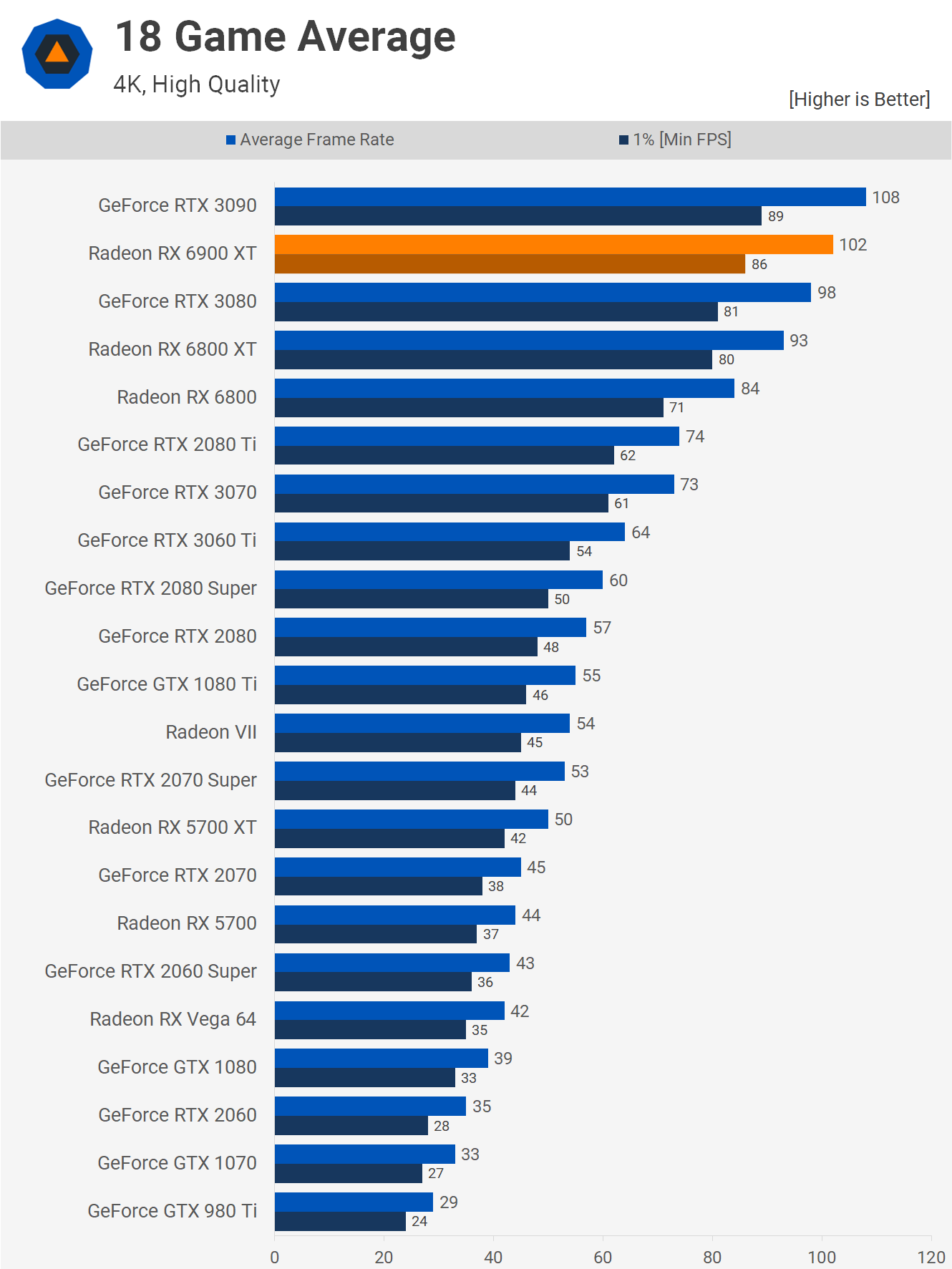
Of course, none of this would matter if the end product wasn’t any good. Despite being an eye-watering $1,000, the Radeon RX 6900 XT offered GeForce RTX 3090 levels of performance, for a $500 smaller price tag. It wasn’t always on-par, and depending on the game and resolution used, the $700 GeForce RTX 3080 was just as fast.
At that price point, AMD had the Radeon RX 6800 XT and the RX 6800 for $50 and $120 less than the RTX 3080, respectively. There was nearly a 30% difference in performance between the 6800 and the RTX 3090, but an enormous 63% difference in price. AMD might not have won the performance crown, but there was no denying the products were still very potent and excellent value for money, at a time when GPU prices were all over the place.
But countering this was the ray tracing performance. In short, it was nowhere near as good as that achieved by Nvidia’s Ampere GPUs, though given that this was AMD’s first dip into the world of physically correct light modeling, the capabilities weren’t surprising.
Where Nvidia chose to design and implement two large, custom ASICs (application-specific integrated circuits) for handling ray-triangle intersection and BVH (bounding volume hierarchy) traversal calculations, AMD chose a more moderate approach. For the latter, there would be no specialized hardware, with the routines being crunched via the Compute Units.
This decision was based on keeping the die size as small as possible. The Navi 21 chip was pretty large at 521 mm2 and while Nvidia was happy to field even larger processors (the GA102 in the RTX 3090 was 628 mm2), adding bespoke units would have pushed the area out a lot more.
In November of the same year, Microsoft and Sony released their new Xbox and PlayStation consoles, both sporting custom AMD APUs (CPU and GPU in the same die), which used RDNA 2 for the graphics side of things, minus the Infinity Cache. With the need to keep these chips as small as possible, it became crystal clear as to why AMD had chosen this particular route.
It was all about improving the financials of its graphics division.
Money and margins matter
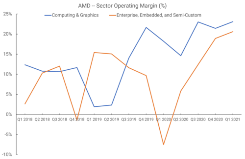
Prior to the second half of 2021, AMD issued its revenue and operating income figures into just two divisions: Computing and Graphics, and Enterprise, Embedded, and Semi-Custom. Revenue from the sales of Graphics cards and discrete GPUs in laptops went into the former, whereas income generated from selling APUs for Xbox and PlayStation consoles went into the latter.
If we look at the period of Q1 2018 through to Q1 2021, we can see that the operating margins were… well… all over the place.
RDNA launched in Q2 2019, but the revenue from such sales would really only start to be felt in the following quarter, as only two models of graphic cards housed the new chip. There’s no way to tell that the rise in operating margins was helped by the GPU architecture, as the figures also include CPU sales.
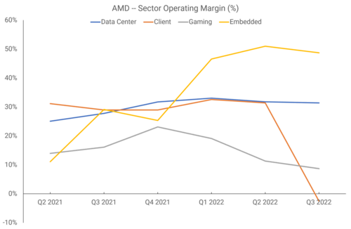
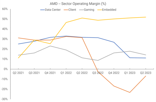
However, from Q2 2021 onward, AMD rejigged the reporting sectors into four divisions: Data Center, Client, Gaming, and Embedded. The third covers everything GPU-related, including the APUs that end up in consoles, and the picture is somewhat clearer.
Now we can see that the margins for AMD’s graphics section have been the weakest of the four. AMD has said that for FY2022, just one customer was responsible for a sixth of the company’s entire revenue, which was surmised by others to be Sony. If that was indeed the case, then sales of the PlayStation 5 APU accounted for over 50% of the Gaming sector’s revenue.
Shipment figures for discrete graphics cards in that financial year took a nosedive, which doesn’t leave much doubt that the operating margins of this division were kept positive by console sales. AMD uses TSMC to manufacture the vast majority, if not all, of its chips but orders have to be placed months in advance – if the processors aren’t sold soon after fabrication, they have to remain in a distribution center, which hurts the margins for that period.
There’s not quite enough information to discern if AMD is making a profit on its investment in RDNA, as it’s not possible to separate the investment in Zen from the Data Center and Gaming margins. But the revenue figures, an average of $1.6 billion for the above 6 quarters, resulted in an average operating margin of 15% – only the Client sector has been lower than this figure and that’s mostly down to the slump in PC sales.
Meanwhile, over the same period, Nvidia’s Graphics segment (which incorporates GPUs for desktops, laptops, workstations, cars, etc) averaged around $3.6 billion per quarter, with a mean operating margin of 43%. The jolly green giant holds a larger market share in the discrete GPU market than AMD, so the larger revenue figure isn’t surprising, but the operating margin is somewhat eye-opening.
But it’s worth taking stock of the fact that the APUs that AMD sells to Microsoft and Sony won’t have large margins anyway, because if they did, there’s no way that you’d be able to buy one of the latest consoles for $400. Mass production of all-in-one chips is good for revenue, but less so for outright profits.
If one removes the estimated revenue that the console chips bring in and assumes that they generate a margin of 10%, this would suggest that RDNA is generating a reasonable amount of profit – the operating margins could be as high as 20%. Not Nvidia-level, but we all know why that company’s margins are so high.
Chiplets and compute
RDNA 2 was certainly an engineering success for AMD, with the design finding a home in almost 50 different products. Financially, though, GPUs were proving to be a constant second-best, compared to the other sectors. At the same time that AMD launched its first update to RDNA, the company also announced a new compute-only architecture, called CDNA.
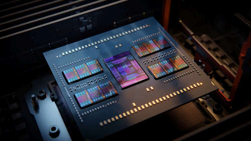
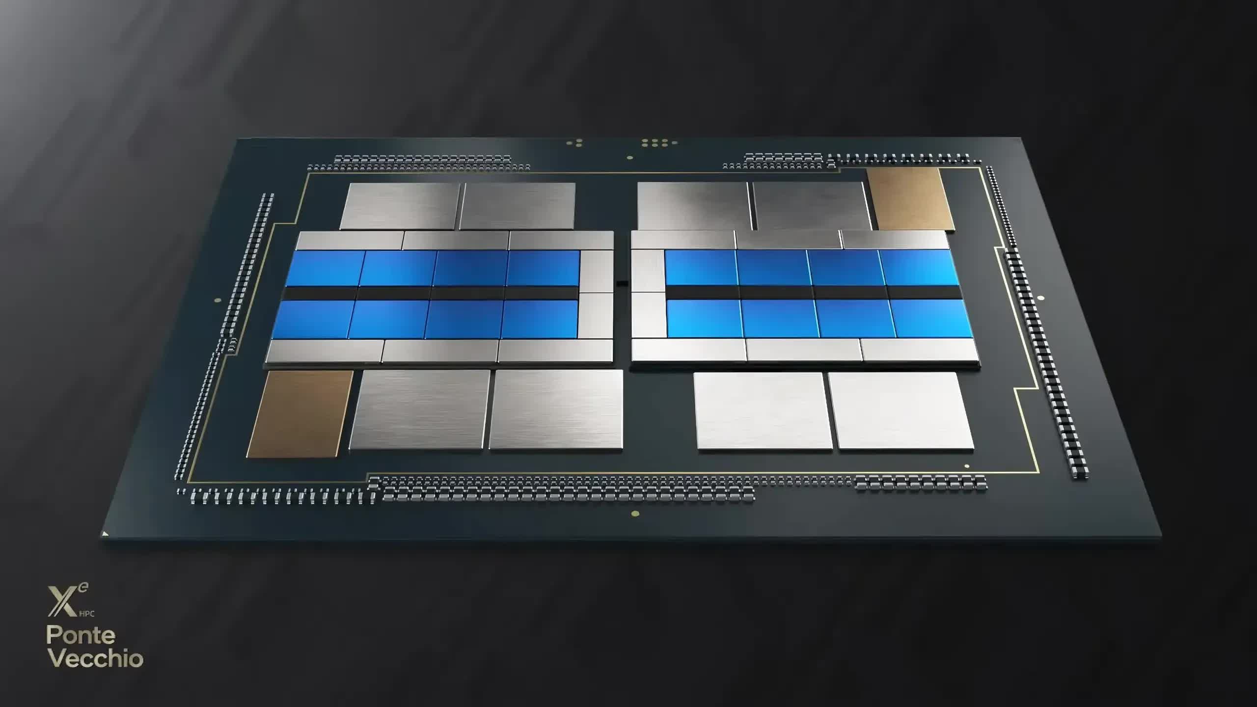
This was GCN-gone-Godzilla, with the first chip to use the design (Arcturus) boasting 128 CUs, in a 750 mm2 die. The Compute Units had been updated to house dedicated matrix units (akin to Nvidia’s Tensor cores) and in the following year, AMD packed two of these enormous processors into a 724 mm2 die. Codenamed Alderbaran (below), it would rapidly become the GPU of choice for many supercomputer projects.
Back in the world of gaming graphics, AMD was looking to leverage more of its CPU expertise. The Infinity Cache in RDNA 2 came about because of the work done in developing a high-density L3 cache and the Infinity Fabric interconnect system for its Zen processors.
So, it was only natural that for RDNA 3, it would use another CPU success: chiplets.
But how to do this? It’s much easier to physically separate cores in central processors because they operate entirely independently. In the vast majority of AMD’s desktop PC, workstation, and server CPUs, you’ll find two at least two so-called chiplets: one that houses the cores (Core Complex Die, CCD) and the other being home to all of the input/output structures (IOD). The main difference between them all is the number of CCDs.
Doing something like this in a GPU is a far harder task. The Navi 21 GPU is a large block of four separate processors, each containing 10 WGPs, rasterizers, render backends, and L1 cache. One might think that these would be ideal for spinning off into discrete chiplets, but the interconnect system required for the huge amount of data transactions would negate any cost savings, and add a lot of unnecessary complexity and power consumption.
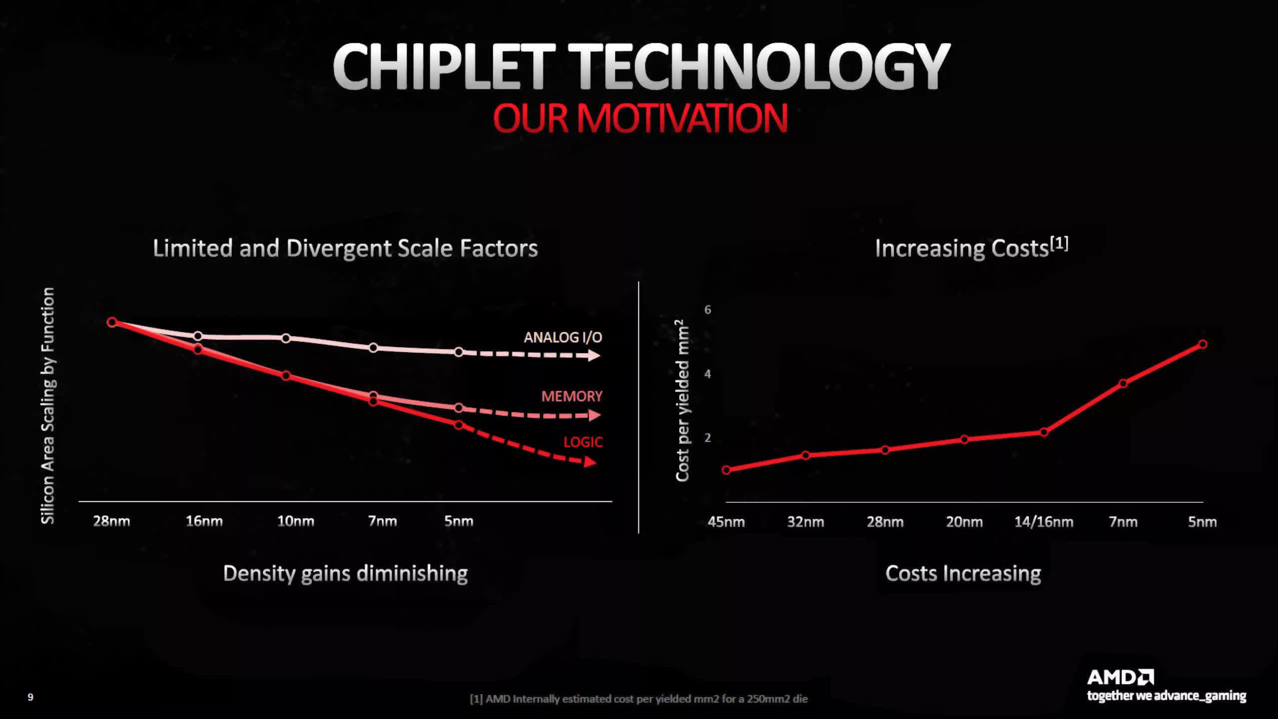
For RDNA 3, AMD took a more measured approach, one born of the limitations that ever-smaller process nodes were struggling against. When the likes of TSMC announce a new manufacturing process, it typically does so with various claims of higher performance, lower power consumption, and greater transistor density.
However, the latter is an overall figure – transistors and other circuitry associated with logic and processing have certainly continued to shrink down in size, but anything to do with signaling and memory hasn’t. SRAM uses an array of transistors to act as a form of volatile memory, but the arrangement can’t be compressed anywhere near as much as logic can.
And as signaling speeds for USB, DRAM, et al all continue to rise, packing these circuits in more closely causes all kinds of interference problems. TSMC’s N5 process node might have a logic density that’s, say, 20% higher than N7, but SRAM and IO circuits are only a few % better.
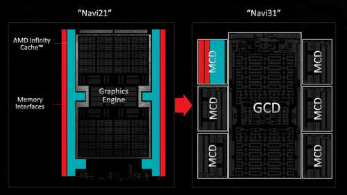
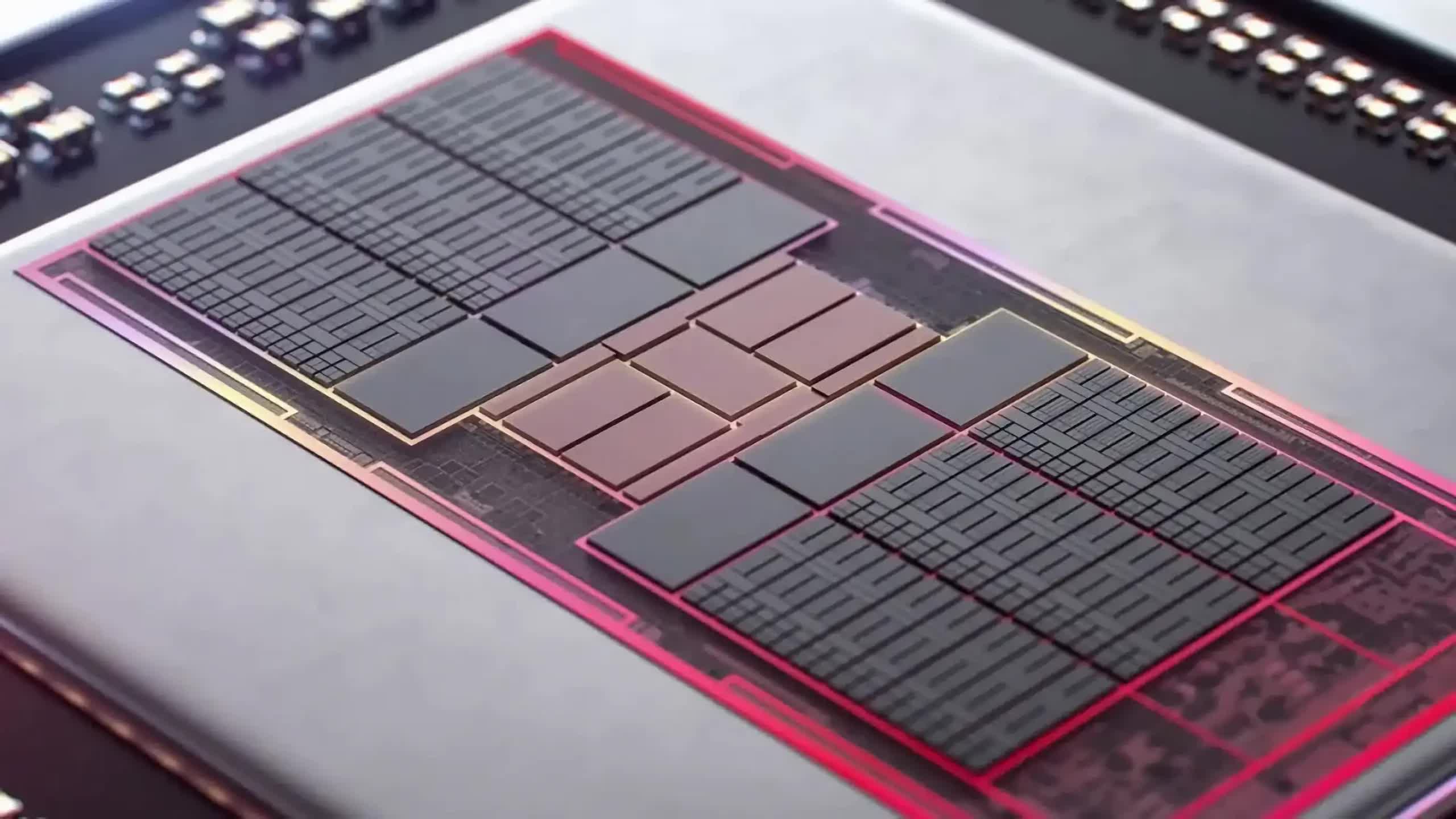
This is why AMD chose to push the VRAM interfaces and L3 Infinity Cache into one chiplet, and the rest of the GPU in another one. The former could be manufactured on a cheaper, less advanced process, whereas the latter could take advantage of something better.
In November 2022, AMD launched RDNA 3 in the form of the Navi 31 GPU. The main chiplet (called a Graphics Compute Die, GCD), was made on TSMC’s N5 process node, and contained 96 Compute Units for a die area of just 150 mm2. Surrounding this were six Memory Cache Dies (MCD), each a mere 31mm2 of silicon, comprising 16 MB of Infinity Cache, two 32-bit GDDR6 interfaces, and one Infinity Link system.
Had AMD chosen to stick with a monolithic approach for the Navi 31, then the entire chip would probably have only been around 500 to 540 mm2 in size, and without the need for a complex network of links between all the chiplets, it would have been cheaper to package it all, too.
AMD had planned all of this for many years, so it had clearly worked the numbers of profitability. It all stems from wafer yields and the increasing costs of chip fabrication. Let’s use some estimated prices to highlight this – a single N6 wafer, used to make the MCDs, might be $12,000 but it would yield over 1,500 of those chiplets ($8 per die). A $16,000 N5 wafer might produce 150 GCDs, at $107 per die.
Combine one GCD with six MCDs and you’re looking at $154 or so before you need to add in the cost of packaging them together. On the other, a single 540 mm2 chip from an N5 wafer might cost around $250, so the cost-benefit of using chiplets is immediately obvious.
Cutting edge meets conservative change
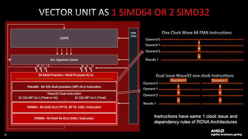
As bold as the use of chiplets for RDNA 3 was, the rest of the updates were more conservative. The register files, and L0, L1, and L2 caches were all increased in size, but the L3 Infinity Cache was reduced. Each SIMD unit was expanded to work on 64 data points at the same time, so wave64 processing was now single cycle.
Ray tracing performance was given a modest boost, with the units given tweaks to improve ray-triangle intersection throughput, but there was no other specialized hardware in this regard. Nor were CDNA’s matrix units copied across to RDNA – such operations were still handled by the Compute Units, although RDNA 3 did sport an ‘AI accelerator’ (AMD has said little about the function of this unit).
Quite a lot of fuss was made over the new design’s processing performance, with the phrase ‘dual issue’ being bandied about. When used, it allows the SIMD units to evaluate two instructions at the same time, and AMD’s marketing division showed this by stating a peak FP32 throughput double that seen with RDNA 2.
The only problem is the ability to carry out dual issuing of instructions is heavily dependent on the compiler (a program in the driver that converts a program’s code into GPU operations) being able to spot when this can take place. Compilers aren’t great at doing this and generally require the input of a trained human eye to get the best results.
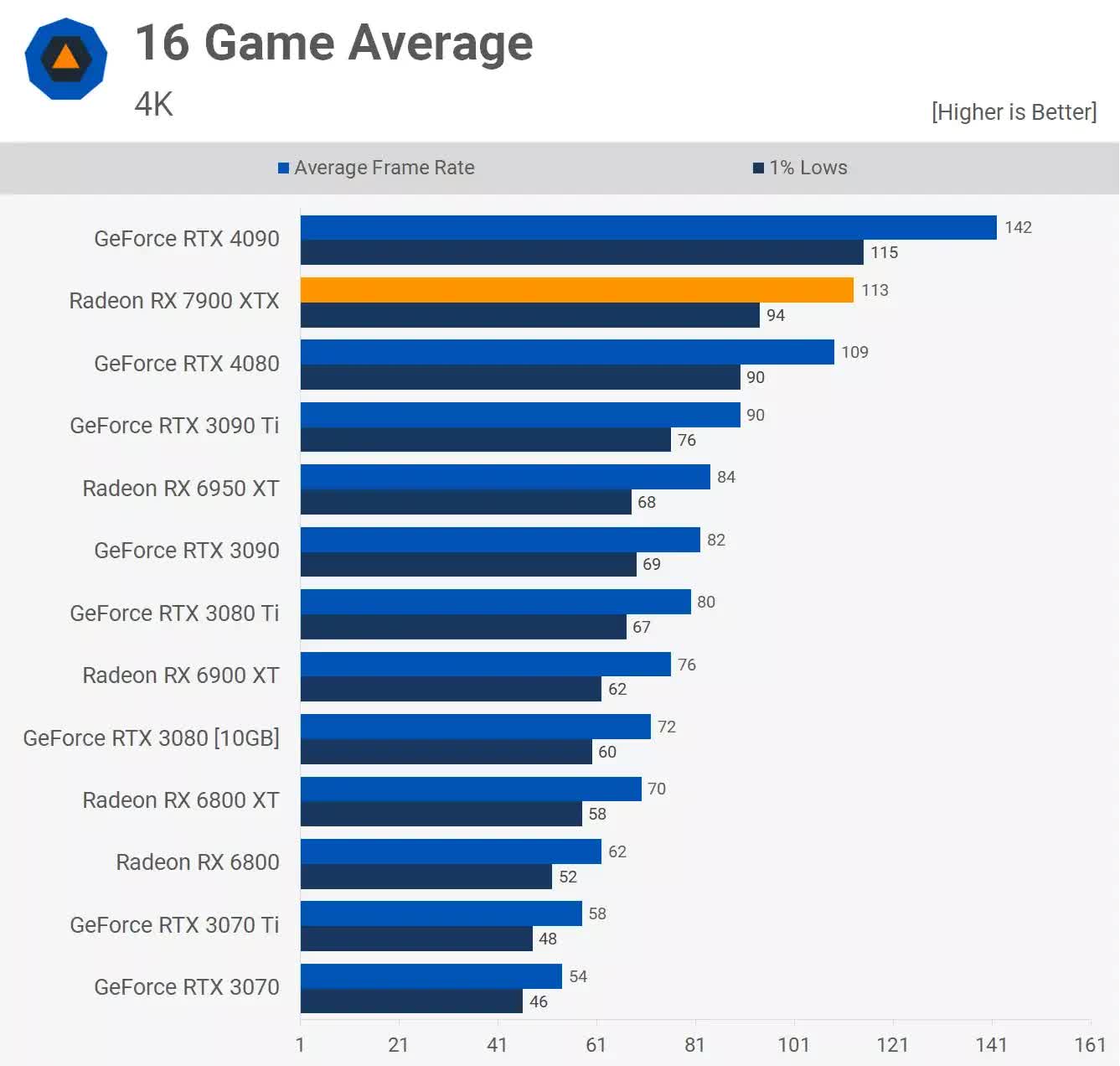
The most powerful card to sport an RNDA 3 chip, the Radeon RX 7900 XTX, was met with praise when it hit the shelves, with a price tag of $1,000. While generally not as fast as Nvidia’s GeForce RTX 4090, it was certainly a match for the RTX 4080 and over the months since then, price cuts from AMD have made it a far better choice.
Ray tracing is, once again, not a strength, and despite claims of improving power efficiency, many people were surprised by how much power the Navi 31 required, especially while idle. While it certainly needed less power than the previous Navi 21, the need for the Infinity Link system partly offset any gains from using the better process nodes.
Something else that was amiss, compared to RDNA 2, was the breadth of the product range. At the time of writing, RDNA 3 can be found in 18 separate products, though market conditions have probably forced AMD’s hand on this matter.
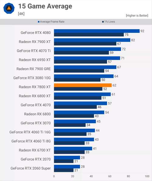
To some, what was even worse was that when the mid-range and low-end RDNA 3 graphics cards finally appeared, their relative performance improvement over the older design was somewhat understated – in the case of the Radeon RX 7800 XT, it was just a few % faster than the outgoing RX 6800 XT.
And the use of chiplets doesn’t seem to have benefited AMD’s operating margins all that much. In the three quarters since RDNA 3 appeared, the Gaming division’s revenue and margins have stayed pretty much as they were. Of course, it’s possible that the new GPUs have actually improved things because if console APU sales have decreased, it would seem that the only way the financials would remain the same would be if GPUs have become more profitable.
However, AMD no longer sells APUs just to Microsoft and Sony. Handheld PCs, such as Valve’s Steam Deck, have been increasingly popular and since all of them sport an AMD chip, these sales will have contributed to the bank balance of the Gaming division.
What the future holds for RDNA
If we take stock of what AMD has achieved with RDNA in four years, and appraise the overall success of the changes, the end result will fall somewhere between Bulldozer and Zen. The former was initially a near-catastrophic disaster for the company but redeemed itself over the years by being cheap to make. Zen, on the other hand, has been outstanding from the start and forced a seismic upheaval of the entire CPU market.
Although it’s too hard to judge precisely how good it’s been for AMD, RDNA and its two revisions are clearly neither of those. Its market share in the discrete GPU sector has fluctuated a little during this time, sometimes gaining ground on Nvidia, and losing at other times, but generally, it has remained the same.
The Gaming division has made a small but steady profit since its inception, and although margins seem to be declining at the moment, there’s no sign of impending doom. In fact, in terms of margins only, it’s AMD’s second-best sector!
And even if it wasn’t, AMD makes more than enough cash from its embedded section (thanks to the purchase of Xilinx) to stave off any short periods of overall loss.
But where does AMD go from here?
There are only three ways forward: the first is to stay on the current course of minor architectural updates, continue to accrue small margins, and hold a narrow slice of the entire GPU market. The second would be to abandon the high-end desktop GPU sector and focus entirely on dominating the budget and low-end markets, by focusing on technologies that further reduce die sizes and increase wafer yields.
The third route is the polar opposite of the second – forget about being the ‘best value for money’ and having an architecture that can scale to every possible level, and do everything to ensure that it’s a Radeon graphics card, not a GeForce one, that sits at the top of every performance chart.
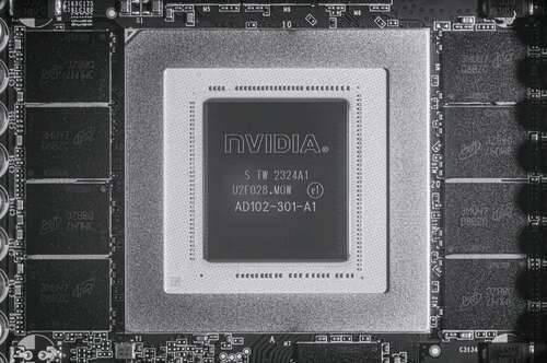
Nvidia achieves this with the RTX 4090 by virtue of using the best possible process node from TSMC and, in terms of shading units, the largest consumer-grade GPU that money can buy. There’s no fancy trickery going on – it’s a brute-force approach and one that works very well. The entire AD103 chip in the RTX 4080 is only 20% larger than the GCD in Navi 31 and it has a reasonably similar performance.
However, RDNA has always been about getting the most from what processing capability is there. The sheer complexity of the cache system in RDNA 2/3 is a testament to this, as both Intel and Nvidia use a far simpler structure in their GPUs.
And speaking of cache, the decision to jam huge amounts of last-level cache into RDNA GPUs to offset the need for ultra-fast VRAM, and boost ray tracing performance, was almost certainly the inspiration for Nvidia to do the same with its Ada Lovelace architecture.
We’re now at a point in the evolution of GPUs where there’s relatively little difference between how different vendors design their graphics processors, and the days of seeing vast improvements in performance from architecture design alone are long gone.
If AMD wants to categorically hold the absolute performance crown, it needs to come up with an RDNA GPU that has considerably more Compute Units than we’re currently seeing. Or just more capable ones – the change in the SIMD units in RDNA 3 is perhaps a sign that in the next revision, we may see CUs sporting four SIMDs rather than two, to remove all of the dual issue limitations.
But even then, AMD needs to have more CUs overall and the only way this can happen is by having a much larger GCD, and this means accepting lower yields or moving this chip to a better process node. Both of these would impact margins, of course, and unlike Nvidia, AMD seems unwilling to push GPU prices through the roof.
It’s also probably unlikely to take the second route, as once this is done, there’s little chance of being able to return. The history of the GPU is littered with companies that have tried, failed, and gone for good once they stopped competing at the top end of the scale.
This leaves option one – carry on with the current course of action. In terms of architecture, Nvidia has significantly reworked its shader cores for a good number of years, and it’s only the past two generations that show lots of similarities. It’s also thrown its considerable resources at developing and marketing machine learning and ray tracing features, with the former being uniquely tied to the GeForce branding.
AMD has developed numerous technologies over the years, but in the RDNA era, none of them have specifically required a Radeon graphics card to utilize them. With its Zen architecture and other CPU inventions, AMD dragged the world of computing into the future, forcing Intel to up its game. It brought power-efficient, multithreaded processing to the masses – not through being the cheaper alternative to Intel, but through competing. and winning, head on.
There’s no denying that RDNA has been a successful design, given how widespread its use is, but it’s certainly no Zen. Being the best value for money or the community favorite with its open-source approach to software isn’t enough if the Gaming sector is to grow. AMD seems to have all of the engineering skills and know-how to make it so; whether they take the plunge is another matter entirely.
Fortune favors the brave, as they say.
