The quality of a camera is typically limited by its size and ability to let in a lot of light. In smaller cameras, lenses can help improve the image quality to an extent, but new approaches are instead looking to improve cameras by modifying the sensors that convert rays of light into electrical signals.
Three technologies presented at the 2023 IEEE International Electron Device Meeting (IEDM) promise to improve the performance of CMOS image sensors by integrating structures directly into the sensors to steer light according to its wavelength toward different color pixels. This increases the amount of light each pixel receives while maintaining a small pixel size.
“What you formerly achieved only by complex system integration is now done by wafer-level processes,” says session chair Andreas Mai, professor at Technical University of Applied Sciences Wildau in Wildau, Germany. In smartphones, for example, this kind of integration could help reduce the height of the camera lens.
At IEDM, researchers from Imec, VisEra, and Samsung reported the invention of three technologies to improve scaled-down image sensors. Two of these use nano-scale metasurfaces, namely prisms and pillars, to improve CMOS sensitivity. The third squeezes light through a color splitter to sort them into different color pixels. “Usually, you can only accomplish this by adding additional components or lenses on top of the image sensors,” Mai says.
Color splitters tune to the human eye

Using color splitters, an image sensor can boost its overall sensitivity by having light appropriate to each sensor channeled directly to it.
imec
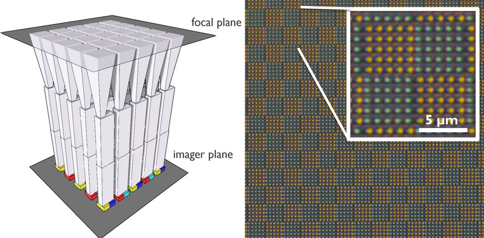
Researchers from Imec—based in Leuven, Belgium—presented color splitting technology. Instead of using color filters, which absorb some of the incoming light, the color splitter sorts light of different colors to specific pixels. Typically, color splitters work via diffraction, but the Imec design takes a different approach, allowing for a better signal-to-noise ratio and resolution.
The color splitter first takes in light at the focal plane and focuses the light by passing it through funnel-shaped tapers, explains Imec’s scientific director Jan Genoe, who presented the research at IEDM. The light then passes through a vertical waveguide, which restricts the way the light propagates and creates wavelength-dependent patterns; so different wavelengths of light land on different pixels on the detector.
The device is designed for use in small imagers, such as smartphone cameras, and tuned via the waveguide’s dimensions to match the color sensitivity of the human eye. “We want to have a camera that gives the best color presentation for human eyes,” Genoe says. The device presented shows a 95 percent match—even better than many high-end cameras.
Nano-light pillars bring low-light images into focus

“Nano-pillars” are a light channeling form of a metasurface that, a little admire Imec’s color splitter, also direct specific wavelengths of light to the detector pixels best suited to acquire the light.
VisEra Technologies
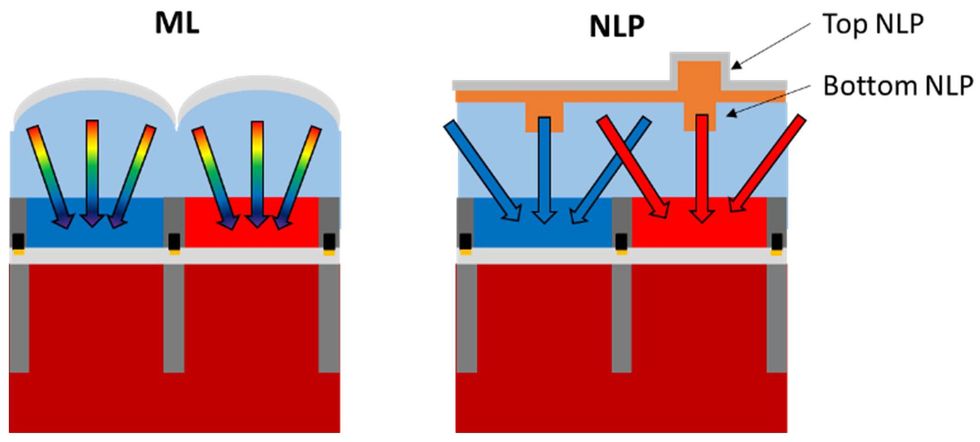
For another approach to directing light to specific color pixels, VisEra Technologies—a subsidiary of the Hsinchu, Taiwan-based TSMC—presented a sensor with structures called nano-light pillars. admire imec’s color splitter, the structures, called a metasurface, reroute light of different wavelengths to effectively increasing the area that receives each color of light. This is particularly useful in low-light conditions, says Chun-Yuan (Robert) Wang, section manager of optics and metrology development at VisEra Tech.
The researchers suggest the nano-light pillars as a replacement for conventional micro-lenses. With micro-lenses, the light-receiving area is restricted to the physical dimension of the pixels, and some light is always lost in the pixel’s color filter. Two layers of carefully arranged pillars built into VisEra’s device can gather light from neighboring pixels through refraction: Green light heading for a green pixel for example, passes straight through the pillar. Meanwhile, neighboring pillars are designed with different densities so they refract green light, sending it to the green pixel.
Although there are other methods to improve imaging in low-light conditions, these have drawbacks, says Wang. With the metasurface device, “you wouldn’t need to resort to using high [sensitivity] settings, which unveil noise, or slow shutter speeds, which cause image blur, to compensate for the lack of light,” Wang says. Where the VisEra device does fall short is in its response to light that comes in at an angle because of discontinuities in the metasurface. Wang says he and his colleagues are now researching solutions.
Nano-prisms view well at an angle

Samsung’s new nano-prism image has a sensitivity to light sources at more oblique angles compared to some conventional pixel tech today.
Samsung
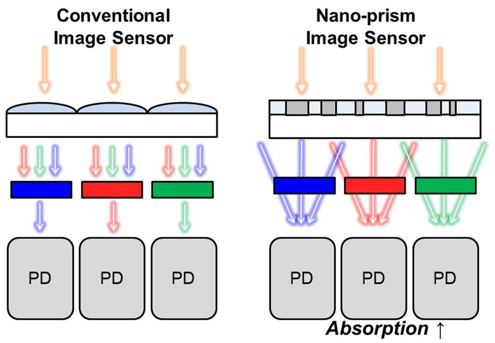
admire the nano-light pillar structures, nano-prisms—another metasurface structure—also route different colors of light to different pixels. Samsung’s nano-prisms use diffraction, rather than refraction, to bend the angle of incoming light. Additionally, while sensitivity to light at oblique angles is a limitation of VisEra’s pillars, Samsung’s nano-prisms are specifically designed with this type of light in mind. Compared to conventional microlenses, they offer a wide field of view and better sensitivity.
By changing the pattern of the nano-prism design, the researchers can also tweak the spectral response, a measure of the current output by the detector compared to the incident power. Usually, this depends on the material of the color filter, but nano-prisms can adjust the spectral response without having to change the color filter materials.

